- 您现在的位置:买卖IC网 > Sheet目录346 > NCP3488DR2G (ON Semiconductor)IC MOSFET DRVR DUAL 12V 8-SOIC
NCP3488
OD
3
V CC
TSD
1
BST
UVLO
IN
2
8
DRVH
FALLING
EDGE
DELAY
MONITOR
7
SWN
FALLING
EDGE
DELAY
MONITOR
START STOP
MIN DRVL
OFF TIMER
NON ? OVERLAP
TIMERS
4
5
6
V CC
DRVL
PGND
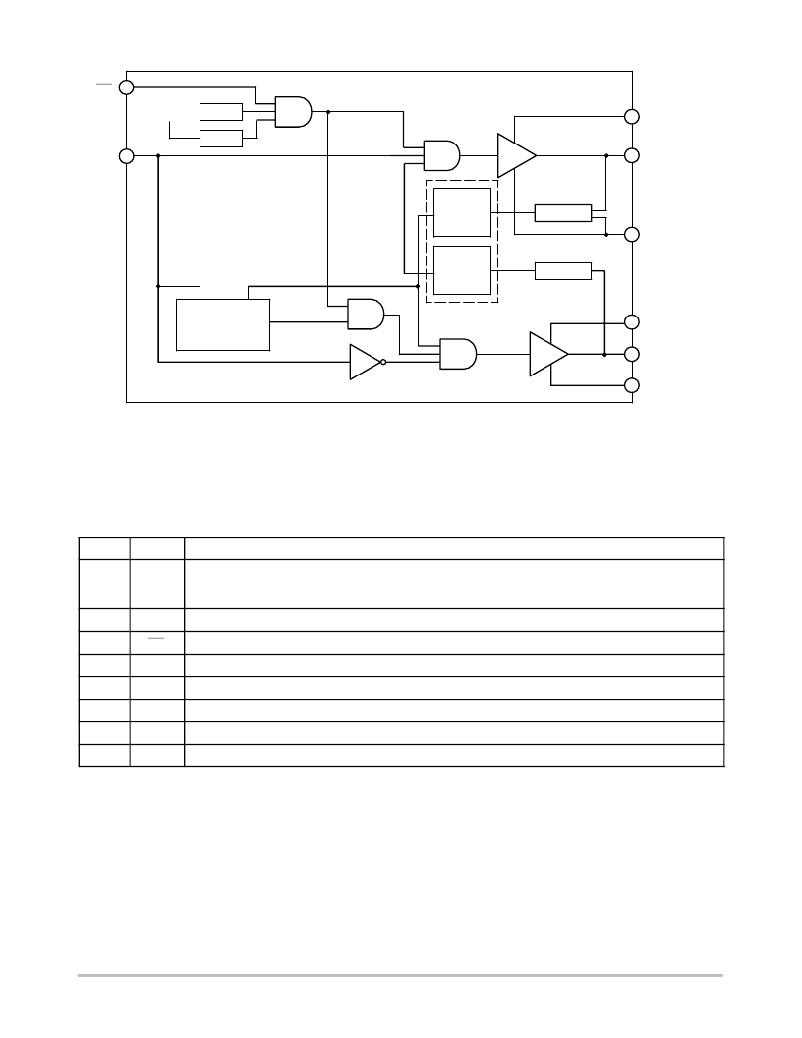
Figure 1. Block Diagram
PIN DESCRIPTION
Pin No.
1
2
3
4
5
6
7
8
Symbol
BST
IN
OD
V CC
DRVL
PGND
SWN
DRVH
Description
Upper MOSFET Floating Bootstrap Supply. A capacitor connected between BST and SW pins holds this
bootstrap voltage for the high ? side MOSFET as it is switched. The recommended capacitor value is between
100 nF and 1.0 m F. An external diode is required with the NCP3488.
Logic ? Level Input. This pin has primary control of the drive outputs.
Output Disable. When low, normal operation is disabled forcing DRVH and DRVL low.
Input Supply. A 1.0 m F ceramic capacitor should be connected from this pin to PGND.
Output drive for the lower MOSFET.
Power Ground. Should be closely connected to the source of the lower MOSFET.
Switch Node. Connect to the source of the upper MOSFET.
Output drive for the upper MOSFET.
http://onsemi.com
2
发布紧急采购,3分钟左右您将得到回复。
相关PDF资料
NCP5007SNT1
IC LED DRIVR WHT COMPACT 5TSOP
NCP5008DMR2
IC LED DRVR WHT BCKLT 10MICROSMD
NCP5010FCT1G
IC LED DRVR WHT BCKLT 8-FLIPCHIP
NCP5021MUTXG
IC WHITE LED DVR HV AMB 16-UQFN
NCP5050MTTXG
IC LED DRIVR PHOTO FLASH 10-WDFN
NCP5111DR2G
IC DRIVER HI/LOW SIDE HV 8-SOIC
NCP5304DR2G
IC DRIVER HI/LOW SIDE HV 8-SOIC
NCP5355DG
IC DRVR SYNC BUCK MOSF 12A 8SOIC
相关代理商/技术参数
NCP348AEMTTBG
功能描述:监控电路 POS OVERVLTG PROTECT CONTROLLER RoHS:否 制造商:STMicroelectronics 监测电压数: 监测电压: 欠电压阈值: 过电压阈值: 输出类型:Active Low, Open Drain 人工复位:Resettable 监视器:No Watchdog 电池备用开关:No Backup 上电复位延迟(典型值):10 s 电源电压-最大:5.5 V 最大工作温度:+ 85 C 安装风格:SMD/SMT 封装 / 箱体:UDFN-6 封装:Reel
NCP348AEMTTBG-CUT TAPE
制造商:ON 功能描述:NCP348AE Series 6.4 V Threshold 28 V Positive Overvoltage Protection Controller
NCP348AEMTTXG
功能描述:监控电路 POS OVERVLTG PROTECT CONTROLLER RoHS:否 制造商:STMicroelectronics 监测电压数: 监测电压: 欠电压阈值: 过电压阈值: 输出类型:Active Low, Open Drain 人工复位:Resettable 监视器:No Watchdog 电池备用开关:No Backup 上电复位延迟(典型值):10 s 电源电压-最大:5.5 V 最大工作温度:+ 85 C 安装风格:SMD/SMT 封装 / 箱体:UDFN-6 封装:Reel
NCP348AEMUTBG
功能描述:监控电路 POSTIVE OVP PRTCTION RoHS:否 制造商:STMicroelectronics 监测电压数: 监测电压: 欠电压阈值: 过电压阈值: 输出类型:Active Low, Open Drain 人工复位:Resettable 监视器:No Watchdog 电池备用开关:No Backup 上电复位延迟(典型值):10 s 电源电压-最大:5.5 V 最大工作温度:+ 85 C 安装风格:SMD/SMT 封装 / 箱体:UDFN-6 封装:Reel
NCP348GEVB
功能描述:电源管理IC开发工具 EVALUATION BRD DEV
RoHS:否 制造商:Maxim Integrated 产品:Evaluation Kits 类型:Battery Management 工具用于评估:MAX17710GB 输入电压: 输出电压:1.8 V
NCP348GEVB
制造商:ON Semiconductor 功能描述:Positive Overvoltage Protection Controll
NCP348MTTBG
功能描述:监控电路 OVER VLTG PROTECTION RoHS:否 制造商:STMicroelectronics 监测电压数: 监测电压: 欠电压阈值: 过电压阈值: 输出类型:Active Low, Open Drain 人工复位:Resettable 监视器:No Watchdog 电池备用开关:No Backup 上电复位延迟(典型值):10 s 电源电压-最大:5.5 V 最大工作温度:+ 85 C 安装风格:SMD/SMT 封装 / 箱体:UDFN-6 封装:Reel
NCP348MTTXG
功能描述:监控电路 POS OVR PROTCT CNTRL RoHS:否 制造商:STMicroelectronics 监测电压数: 监测电压: 欠电压阈值: 过电压阈值: 输出类型:Active Low, Open Drain 人工复位:Resettable 监视器:No Watchdog 电池备用开关:No Backup 上电复位延迟(典型值):10 s 电源电压-最大:5.5 V 最大工作温度:+ 85 C 安装风格:SMD/SMT 封装 / 箱体:UDFN-6 封装:Reel
